8:00 - 17:30
Monday to Saturday
Monday to Saturday
Thermal Stability
Ceramic materials excel in high-temperature applications because they dissipate heat effectively and maintain structural stability under variable temperatures.
Insulation
Ceramic offers superb insulation, which means heat is less likely to pass through the substrate. This keeps the components on the circuit board safe from damage.
Inorganic Nature
Due to its inorganic composition, ceramic lasts longer and resists chemical erosion. This durability ensures functionality over extended periods without degradation.
Multi-Layering
Multi-layer ceramic PCBs enable more complex circuit designs. Ceramic’s robustness ensures the safety of other components even with the addition of layers.
Introduction to Ceramic PCB
If you’re working on demanding electronic applications that require high performance and reliability, consider using Ceramic PCBs. Unlike traditional boards made from fiberglass or epoxy, Ceramic PCBs use ceramic materials, offering unique properties and capabilities. They are suitable for environments that demand high thermal conductivity, high-frequency electrical performance, and durability in harsh conditions.
Because they handle higher temperatures and offer better thermal conductivity, Ceramic PCBs are ideal for power electronics, aerospace, and military applications. When you’re selecting a PCB fabricator, think about factors like cost, materials, and delivery time. At PCBAIR, we follow the latest IPC standards and DFM rules to ensure your next Ceramic PCB design meets your needs.
Ceramic PCB Manufacturing
Ceramic PCBs consist of a single ceramic substrate with copper layers applied to both the top and bottom. These copper layers are added through processes like sputtering, plating, sintering, or brazing.
Depending on the ceramic material you need, we offer AlN, alumina, SiC, Si₃N₄, BeO, and hybrid ceramic PCBs. We also provide different types based on the manufacturing process, including LTCC, HTCC, DPC, DBC, thick-film, thin-film, and AMB.
In our ceramic PCB fabrication process, we use two lamination methods to meet your specific requirements: normal lamination and sintering lamination.
In normal lamination, we bond two ceramic substrate layers under high temperature and pressure using a dielectric layer (PP), mainly composed of phenolic, epoxy resin, or specialized thermally conductive materials.
Sintering lamination, also performed under high temperature and pressure, causes the molecules at the contact surfaces of the two ceramic layers to migrate and fuse, forming a dense polycrystalline ceramic with a relative density exceeding 98%.
While normal lamination offers lower manufacturing costs, it significantly reduces the overall thermal conductivity of the ceramic circuit board, and its bonding strength isn’t as high as that of sintering lamination.
If your application demands high thermal conductivity and strong bonding strength, we recommend the sintering lamination method. This technique creates a strong and reliable bond between the copper and ceramic materials without affecting the ceramic substrate’s properties, especially its thermal conductivity and flatness.
Our team is ready to help you determine the best lamination method for your specific needs, ensuring that your ceramic PCBs meet all your performance requirements.
Why Choose Us as Your Ceramic PCB Manufacturing Partner?
PCBAIR has over 10 years of experience in ceramic PCB design and manufacturing. We have a vast network of upstream and downstream resources in the circuit board industry, enabling us to deliver timely and efficient ceramic PCB manufacturing and assembly services to our customers. We can also provide oxidation-free ceramic PCBs that can withstand harsh environments for extended periods.
Competitive Pricing
With over 10 years in the PCB industry, PCBAIR has established a reliable supply chain that ensures access to premium components at competitive prices. For complex projects needing special materials or advanced technical specifications, our strong manufacturing capabilities enable us to provide cost-effective solutions while maintaining high quality.
Fast and Reliable Delivery
We ensure rapid production times, with samples shipped within 24-48 hours and mass production orders delivered within 72-120 hours. Our partnerships with global logistics providers like UPS, EMS, FedEx, DHL, and TNT guarantee prompt and reliable shipping, supported by our digitalized factory management and 90% automation for enhanced efficiency.
Quality Assurance
Our rigorous quality inspection begins with incoming material checks. We use AOI to detect defects and X-ray to identify internal issues. Electrical performance testing is performed with advanced automatic test machines and flying probe testers. Before shipment, our dedicated QC team conducts a thorough manual visual inspection to ensure all products meet strict quality standards.
Customer Service
Our experienced sales, order management, and engineering teams provide expert support throughout your project. The sales team handles support and project follow-ups, while the order management team ensures timely quotations and monitors production status. Our engineering team reviews your design files, offering professional advice to optimize production efficiency.
PCB Laminate Materials Suppliers
To ensure your PCBs are reliable and perform well, we use high-quality laminate materials. We have built strong partnerships with top suppliers in the industry, including trusted brands like Rogers, Panasonic, Dupont, Arlon, Taconic, Nelco, Isola, Teflon, and more. This means you receive the best materials tailored to your project needs, providing the performance and durability you expect.

Ceramic PCB Capabilities
By reviewing the following ceramic PCB capabilities table, you can briefly understand what we can do.
| Specification | Capabilities |
|---|---|
| ceramic substrate | Al₂O₃ (alumina) / SiC / BaTiO₃ / AlN (aluminum nitride) / Si₃N₄ (silicon nitride) / ZrO₂ / BeO |
| Layer | 1-6L |
| Thicker Copper | 1/3OZ-12OZ |
| Solder Mask | Green / White / Red / Black / Blue / Yellow |
| Finished Surface | OSP / HASL / LF HASL / Immersion Silver / Immersion Gold / Nickel Palladium |
| Finished Board Thickness | 0.15~5.0mm |
| Copper Thickness | 2-210um |
| Minimum Hole Size | 4mil (0.1mm) |
| Hole Offset Tolerance | Length and width ±0.1mm, Thicknesses ±0.05mm |
| Trace Width/Space | ≥50/50um |
| Heat Resistance | 350±10℃, 15min No peeling and explosion (IPC-TM-650 2.4.7) |
| Maximum Size | 138*190 (Customizable maximum size 160*280) |
| Weldability | >95% (IPC-TM-650 2.4.14) |
| Copper foil Peel Strength | >2 (IPC-TM-650 2.4.8) N/mm |
Need Help With Your Project?
Please send us a message, and our ceramic PCB manufacturing capabilities can help you complete your next project.
Ceramic PCB Samples We Manufacture for Our Customers
We have obtained a variety of certifications and registrations, including ISO 9001, automotive and medical certifications, as well as SGS and UL certifications, and we maintain rigorous quality control through IQC, IPQC, and OQA. We deliver high-quality ceramic PCBs on schedule and within budget with outstanding precision.


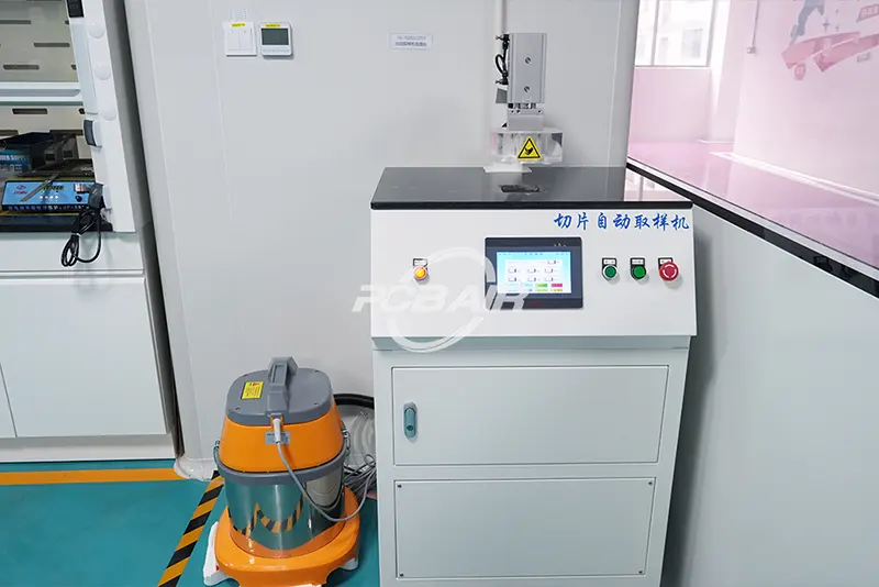
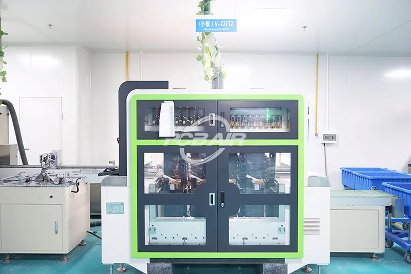
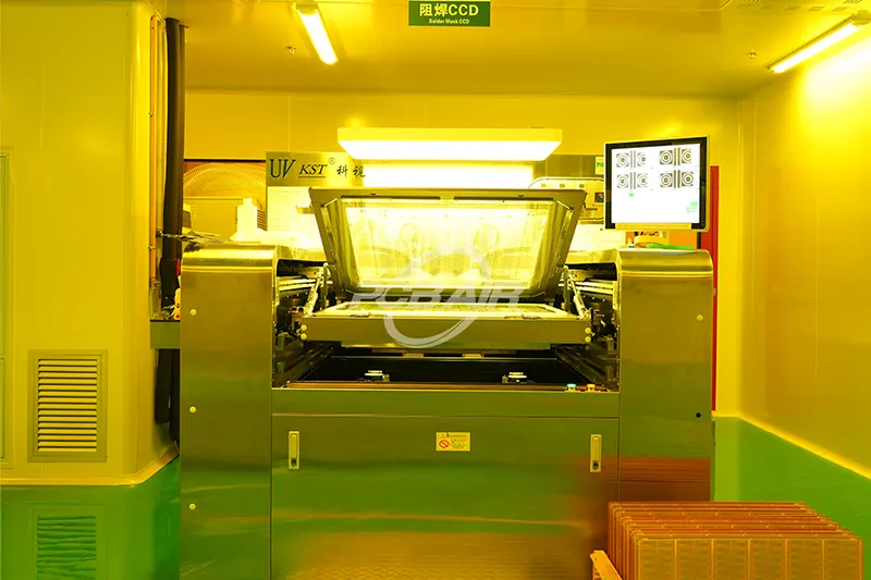
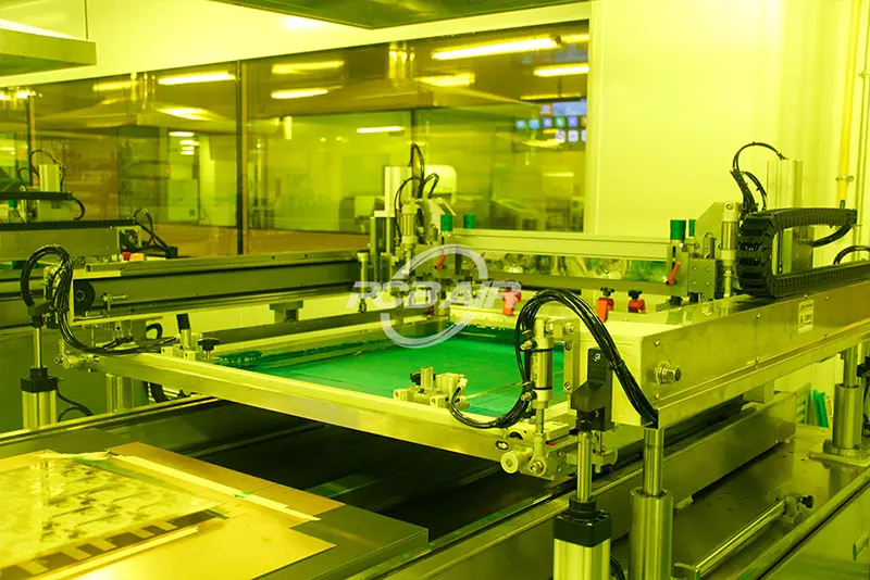
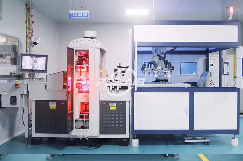
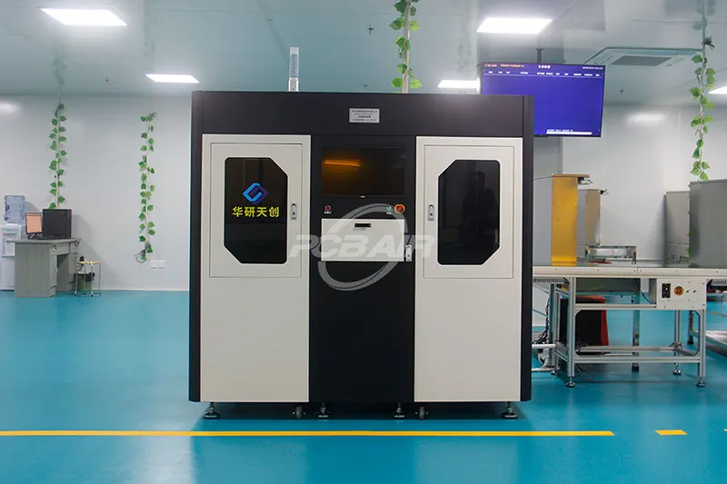
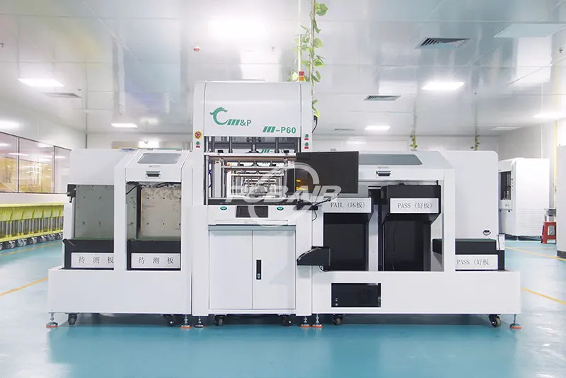
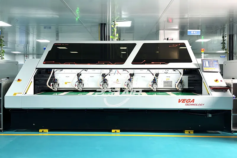
Ceramic PCB Manufacturing Equipment
Our 65,000 sqft campus in Shenzhen, China contains the advanced equipment required for the manufacture and assembly of your PCBs. Our precision milling and laser cutting machines handle the toughness of ceramic materials, ensuring clean and accurate edges every time. We use carbide and diamond-coated drill bits for exact drilling, preserving the integrity of your ceramic substrates.
Additionally, automated assembly lines streamline production, while testing equipment verifies each electrical connection and structural detail. This ensures we deliver ceramic PCBs that meet your exact specifications and comply with stringent quality standards.