8:00 - 17:30
Monday to Saturday
Monday to Saturday
Conductivity
Gold fingers provide excellent electrical conductivity, reducing signal loss, thus ensuring reliable performance for high-speed data transfer.
Corrosion
Gold resists corrosion and oxidation, keeping connections intact over time. Device lifespan extends, reducing failures in harsh conditions.
Signal Quality
Smooth, gold-plated contacts reduce contact resistance, preserving signal quality. Fast data transfers in modern electronics are supported.
Wear Resistance
A thin gold layer over nickel provides wear resistance during repeated insertions, extending PCB and connector lifespan despite gold’s softness.
Introduction to Gold Finger PCB
Gold fingers are typically plated with 5 to 30 microns of hard gold. Hard gold offers excellent wear resistance and can withstand up to 20,000 insertions without quality degradation when the thickness exceeds 5 microns. However, applying hard gold is a complex process that consumes more gold, leading to higher costs.
For many PCBs that don’t require frequent insertion, thick or hard gold plating isn’t necessary. You can opt for immersion gold plating (soft gold) with a thickness of 1 to 3 microns, effectively reducing the PCB’s purchase price without compromising functionality.
At PCBAIR, we perform all gold finger processes in-house and offer gold thickness options ranging from 2 to 50 microns, so you can specify your exact requirements. We ensure quality and reliability by conducting 100% E-tests and AOI inspections on all PCB gold fingers.
Gold Finger PCB Manufacturing & Plating Process
Reliable gold finger PCB manufacturing delivers stable performance for demanding applications. Choosing high-performance FR4 substrates helps maintain durability and reliability throughout the product’s lifespan. Precisely engineered dimensions—length, width, and spacing—ensure each gold finger meets industry standards. Beveling the edges at a 45-degree angle ensures smooth insertion into connectors and reduces wear during repeated use.
Surface preparation is important for achieving a high-quality plating outcome. We clean the PCB surface thoroughly to remove any contaminants that could affect adhesion. Advanced methods, such as chemical treatment and plasma etching, ensure the surface is ready for plating. The process begins with applying a nickel layer to the exposed copper areas of the gold fingers. This nickel layer acts as a protective barrier, preventing copper migration and ensuring strong adhesion for the gold plating.
The gold plating stage is carried out with accuracy to achieve good conductivity and oxidation resistance. We strictly control the thickness of both nickel and gold layers to ensure reliable electrical connections and extended product life. Typically, 3-6 microns of nickel and 1-2 microns of gold are applied, following industry best practices to balance durability with cost efficiency.
Quality control procedures include detailed inspection of the gold fingers for uniformity, surface integrity, and appropriate plating thickness. Using advanced microscopes and specialized testing equipment, we verify compliance with specifications and identify any defects. Electrical testing is also conducted to confirm conductivity and signal integrity, ensuring the boards meet all performance requirements before final assembly.
Commitment to quality is evident at every stage of the manufacturing process. Experience and attention to detail lead to a product that meets the high-performance standards expected by our customers.
Why Choose Us as Your Gold Finger PCB Manufacturing Partner?
PCBAIR is a leading PCB manufacturer in China. We produce gold finger PCBs that meet industry standards. We offer a gold plating process up to 50µm thick and handle PCBs ranging from single-sided to 40 layers, including rigid, flexible, and rigid-flex boards. All gold finger process is done in-house and undergo 100% E-test, AOI inspection, and visual inspection to ensure product quality.
Competitive Pricing
With over 10 years in the PCB industry, PCBAIR has established a reliable supply chain that ensures access to premium components at competitive prices. For complex projects needing special materials or advanced technical specifications, our strong manufacturing capabilities enable us to provide cost-effective solutions while maintaining high quality.
Fast and Reliable Delivery
We ensure rapid production times, with samples shipped within 24-48 hours and mass production orders delivered within 72-120 hours. Our partnerships with global logistics providers like UPS, EMS, FedEx, DHL, and TNT guarantee prompt and reliable shipping, supported by our digitalized factory management and 90% automation for enhanced efficiency.
Quality Assurance
Our rigorous quality inspection begins with incoming material checks. We use AOI to detect defects and X-ray to identify internal issues. Electrical performance testing is performed with advanced automatic test machines and flying probe testers. Before shipment, our dedicated QC team conducts a thorough manual visual inspection to ensure all products meet strict quality standards.
Customer Service
Our experienced sales, order management, and engineering teams provide expert support throughout your project. The sales team handles support and project follow-ups, while the order management team ensures timely quotations and monitors production status. Our engineering team reviews your design files, offering professional advice to optimize production efficiency.
PCB Laminate Materials Suppliers
To ensure your PCBs are reliable and perform well, we use high-quality laminate materials. We have built strong partnerships with top suppliers in the industry, including trusted brands like Rogers, Panasonic, Dupont, Arlon, Taconic, Nelco, Isola, Teflon, and more. This means you receive the best materials tailored to your project needs, providing the performance and durability you expect.

Gold Finger PCB Capabilities
By reviewing the following gold finger PCB capabilities table, you can briefly understand what we can do.
| Specification | Capability |
|---|---|
| Material | FR4 (Rogers, Shengyi, Tuc, KB, Panasonic) |
| Layer | 1-40L |
| Board Thickness | 0.6-8mm |
| Board Thickness Tolerance | ±5% |
| Minimum PCB Size | 2.5×2.5mm (need to create panel), 10x10mm (can do single board) |
| Maximum PCB Size | 500x1500mm |
| Maximum Copper | 6OZ |
| Gold Thickness | Hard Gold: 5 to 50µ”, ENIG: 1 to 4µ” |
| Finished Surface | HASL, LF HASL, ENIG, Hard Gold, OSP, ENEPIG |
| Solder Mask | Green, Red, Yellow, Blue, White, Black, Pink, Purple, Matte Black, Matte Green |
| Silkscreen | Red, Yellow, White, Black |
| Minimum Laser Drill | 0.075mm |
Need Help With Your Project?
Please send us a message, and our gold finger PCB manufacturing capabilities can help you complete your next project.
Gold Finger PCB Samples We Manufacture for Our Customers
We have obtained a variety of certifications and registrations, including ISO 9001, automotive and medical certifications, as well as SGS and UL certifications, and we maintain rigorous quality control through IQC, IPQC, and OQA. We deliver high-quality gold finger PCBs on schedule and within budget with outstanding precision.


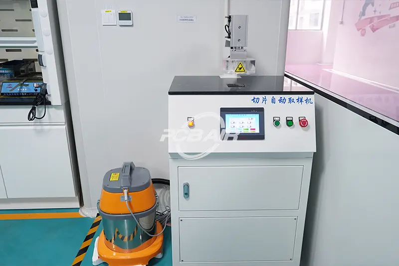
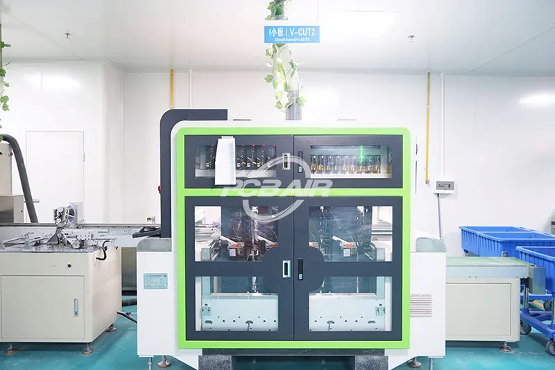
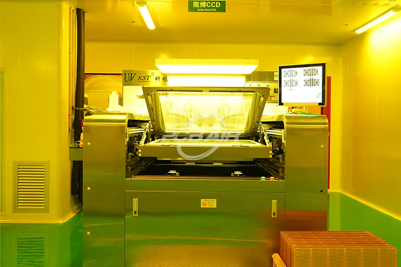
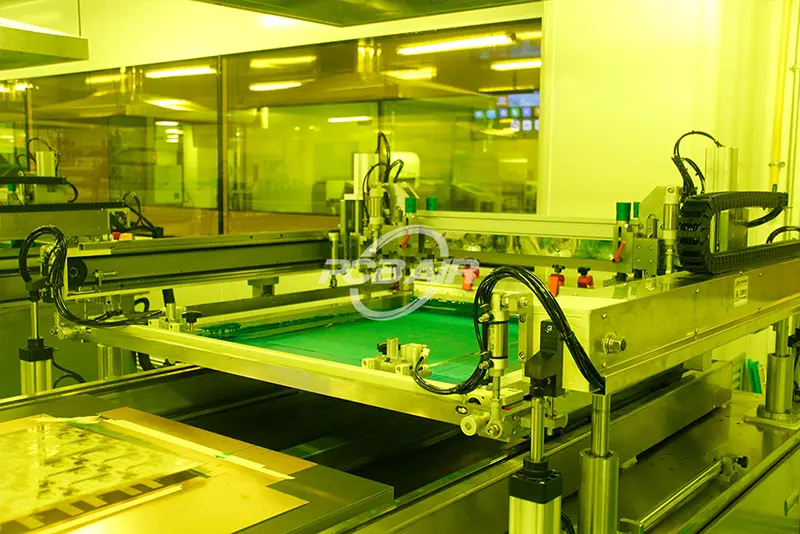
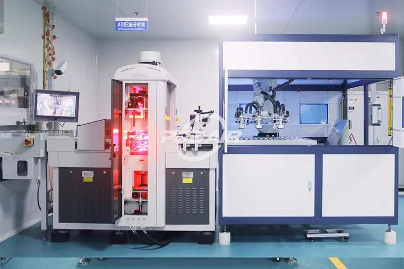
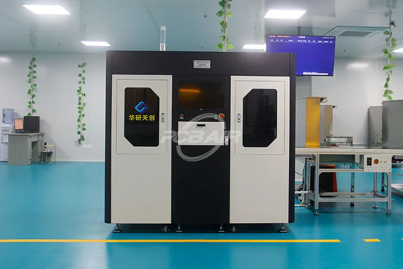
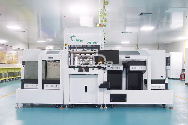
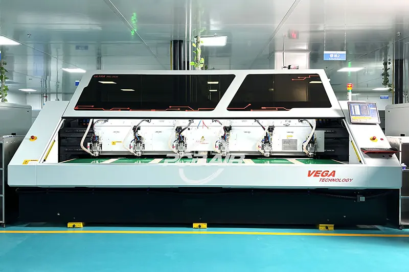
Gold Finger PCB Manufacturing Equipment
Our 65,000 sqft campus in Shenzhen, China contains the advanced equipment required for the manufacture and assembly of your PCBs. By using CNC drilling and routing machines, we achieve precise hole placement and accurate board dimensions. Our nickel and gold plating equipment provides high-quality finishes on edge connectors, enhancing conductivity and durability.
Beveling machines shape PCB edges for smooth connector insertion. Electroplating equipment applies uniform layers of copper, nickel, and gold. We use AOI machines for early defect detection and testing equipment to verify PCB functionality, guaranteeing compliance with your specifications.