8:00 - 17:30
Monday to Saturday
Monday to Saturday
Structure
Thicker copper makes PCBs rigid, reducing flex and vibration. Heavy copper enables higher density with fewer layers, fitting conductive material into less space.
High Current
Heavy copper PCBs can save you space and money by replacing bulky cable harnesses. You can integrate both high and low current components on the same board.
Material
Choosing a base material that suits your application’s operating temperature is important. Consider options like High Tg FR4, BT Epoxy, or GPY Polyimide.
Heat Dissipation
Heavy copper helps conduct heat to the edges of your board, boosting performance. Copper-plated vias carry high current and efficiently transfer heat to external heat sinks.
Introduction to Heavy Copper PCB
Heavy Copper PCBs, with copper thicknesses from 4oz/ft² to 20oz/ft², are important for handling heavy currents and dissipating heat effectively. Standard PCBs can’t manage the high I²R heat losses from large currents, leading to overheating and failure. Heavy Copper PCBs have lower-resistance traces that carry heavy currents and transfer heat away, ensuring reliable performance in high-current applications.
PCBAIR has extensive experience in heavy copper PCB fabrication, offering selectively thicker copper on the same layer. We offer custom fabrication to meet your specific design needs, encompassing varying copper thicknesses, board dimensions, layer counts, and other specifications. Our heavy copper PCBs feature high-precision etching, tight tolerances, uniform ink thickness, optimal protection, and a bright finish. From design analysis (DFM, DFT, and DFA) to dedicated engineering support, we partner with you throughout your project, from prototype to volume production.
Heavy Copper PCB Manufacturing
Thick copper PCBs are the ideal solution for applications requiring high cooling, current, and power. While they come at a premium compared to standard boards due to increased material costs and the specialized equipment and knowledge required for heavy copper PCB manufacturing, the performance gains are often worth it. Standard PCB fabrication processes are inadequate for heavy copper. Trying to use them leads to over etched margins and uneven trace sidewalls. Heavy copper necessitates specialized etching and plating techniques for clean edges and electroplating to thicken plated through-hole walls.
When designing with heavy copper, pay attention to your substrate. Options range from standard FR-4 (130°C operating temperature) to advanced, high Tg materials. The right substrate is key. High current can cause cracks and delamination if the Tg of the copper and substrate aren’t compatible. You need a material with low TCE (thermal coefficient of expansion) to prevent this, along with high CTI and CAF resistance. A high Tg is also important for handling the mechanical stress on those plated through-holes.
We use a laminated deposition process for heavy copper PCB manufacturing. This process uses heavy base copper in plating and etching systems, achieving precise track edges, finer lines, and tighter spacing. It makes demanding heavy copper applications practical and cost-effective.
Why Choose Us as Your Heavy Copper PCB Manufacturing Partner?
With over 10 years of experience in heavy copper PCB design and manufacturing, PCBAIR adheres to stringent quality standards: all our products are ISO 9001 certified, UL certified, RoHS compliant, and meet IPC Class 2 standards for PCB manufacturing. To ensure high quality and reliability, our PCBs undergo rigorous inspections, including FAI, AOI, X-ray inspection, FQA, and functional testing, guaranteeing defect-free heavy copper PCBs that meet your specific requirements.
Competitive Pricing
With over 10 years in the PCB industry, PCBAIR has established a reliable supply chain that ensures access to premium components at competitive prices. For complex projects needing special materials or advanced technical specifications, our strong manufacturing capabilities enable us to provide cost-effective solutions while maintaining high quality.
Fast and Reliable Delivery
We ensure rapid production times, with samples shipped within 24-48 hours and mass production orders delivered within 72-120 hours. Our partnerships with global logistics providers like UPS, EMS, FedEx, DHL, and TNT guarantee prompt and reliable shipping, supported by our digitalized factory management and 90% automation for enhanced efficiency.
Quality Assurance
Our rigorous quality inspection begins with incoming material checks. We use AOI to detect defects and X-ray to identify internal issues. Electrical performance testing is performed with advanced automatic test machines and flying probe testers. Before shipment, our dedicated QC team conducts a thorough manual visual inspection to ensure all products meet strict quality standards.
Customer Service
Our experienced sales, order management, and engineering teams provide expert support throughout your project. The sales team handles support and project follow-ups, while the order management team ensures timely quotations and monitors production status. Our engineering team reviews your design files, offering professional advice to optimize production efficiency.
PCB Laminate Materials Suppliers
To ensure your PCBs are reliable and perform well, we use high-quality laminate materials. We have built strong partnerships with top suppliers in the industry, including trusted brands like Rogers, Panasonic, Dupont, Arlon, Taconic, Nelco, Isola, Teflon, and more. This means you receive the best materials tailored to your project needs, providing the performance and durability you expect.

Heavy Copper PCB Capabilities
By reviewing the following heavy copper PCB capabilities table, you can briefly understand what we can do.
| Specification | Capabilities |
|---|---|
| Material | FR-4, High Tg |
| Layer | 1-30 |
| Board Thickness | 0.7-8mm |
| Trace Width/Space | 8-12OZ 20/20mil, 14-18oz 25/25mil |
| Minimum PCB Size | 2.5×2.5mm (need to create panel), 10x10mm (can do single PCB) |
| Maximum PCB Size | 500x1500mm |
| Maximum Copper | 36OZ |
| Finished Surface | ENIG / Hard Gold / ENEPIG |
| Solder Mask | Green / Red / Yellow / Blue / White / Black / Pink / Purple / Orange / Gray |
| Silkscreen | White, Black |
| Extra Techniques | Gold fingers, Blind/Buried vias |
| Testing | Fly Probe Testing, AOI testing |
Need Help With Your Project?
Please send us a message, and our heavy copper PCB manufacturing capabilities can help you complete your next project.
Heavy Copper PCB Samples We Manufacture for Our Customers
We have obtained a variety of certifications and registrations, including ISO 9001, automotive and medical certifications, as well as SGS and UL certifications, and we maintain rigorous quality control through IQC, IPQC, and OQA. We deliver high-quality heavy copper PCBs on schedule and within budget with outstanding precision.


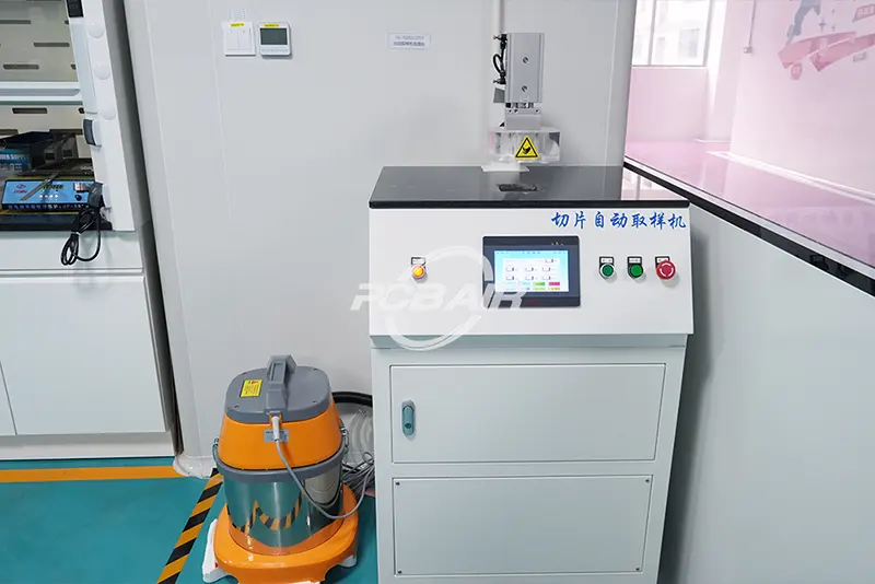
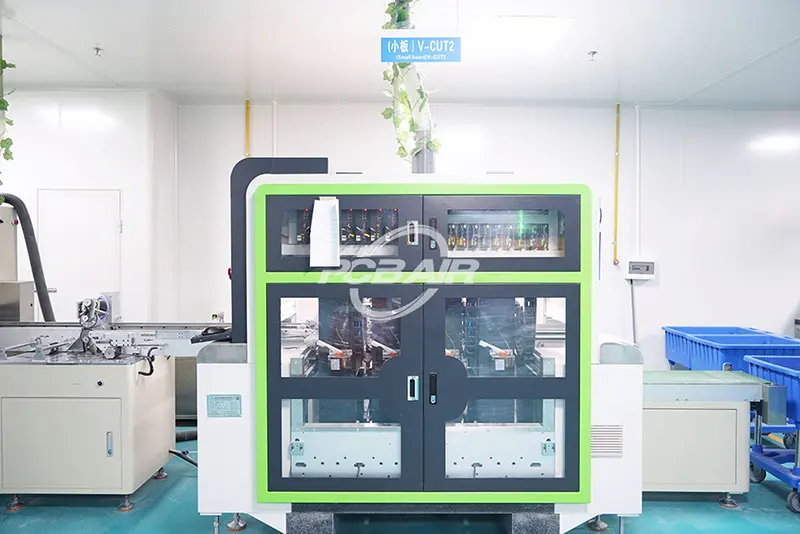
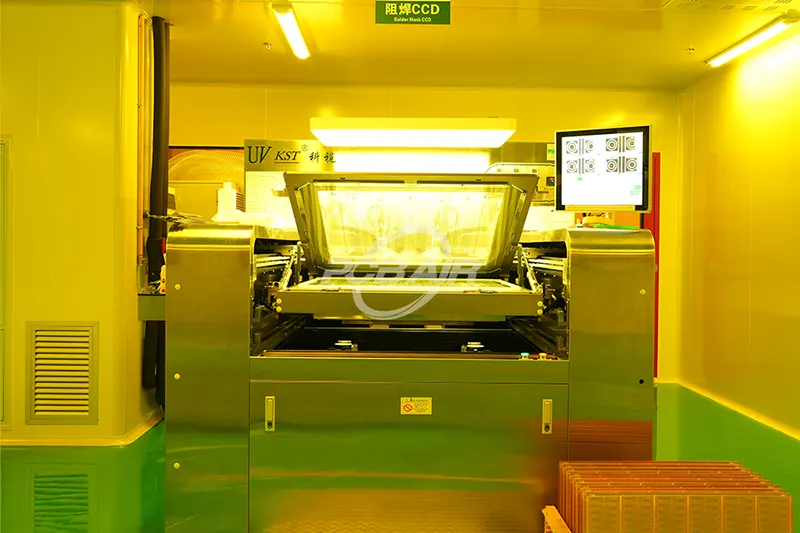
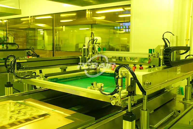
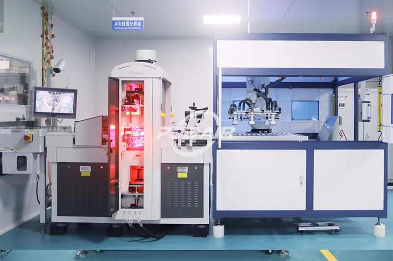
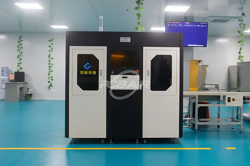
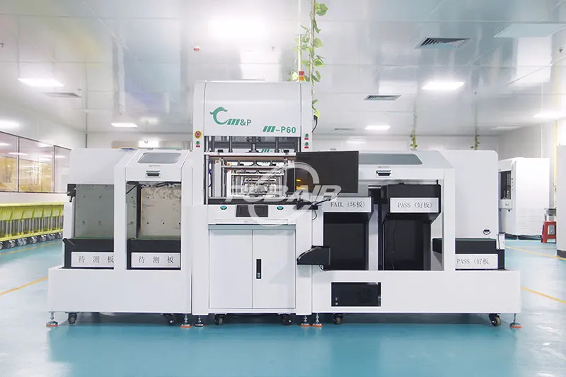
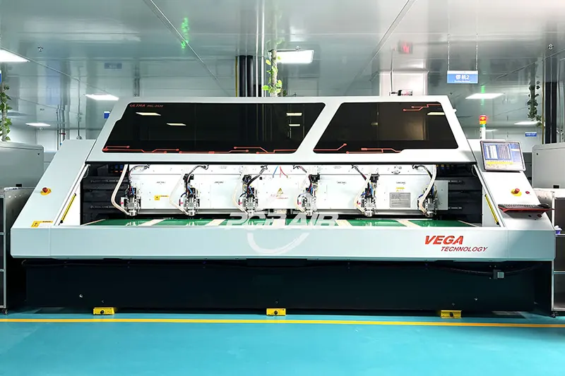
Heavy Copper PCB Manufacturing Equipment
Our 65,000 sqft campus in Shenzhen, China, houses the advanced equipment required for the manufacture and assembly of your PCBs. Our electrolytic copper plating machines deposit thick copper layers on PCB substrates. A uniform copper deposition is maintained with plating baths and power supplies that provide a stable current and the proper chemical environment. For circuit patterns, we use chemical etching equipment with specialized etchants and control systems to prevent over-etching, important for thick copper PCBs. When precision or complex patterns are required, laser etching machines handle the task.
To ensure structural integrity, our PCB lamination presses bond multiple layers using heat and pressure. High-speed drilling machines create accurate holes, especially plated through holes (vias), with the precision and durability required for thick copper PCBs.