8:00 - 17:30
Monday to Saturday
Monday to Saturday
Smaller Sizes
Higher wiring density fits more components on smaller PCBs. Slim smartphones and wearables become more portable without losing functionality.
Signal Integrity
HDI PCBs use thin lines and close wiring for fast, reliable signals. Vias shorten paths and reduce reflections, ensuring smooth performance.
Better Reliability
Microvias and sequential lamination enhance HDI board performance. More transistors in tight spaces boost speed and efficiency, reducing signal loss and delays.
Cost Savings
HDI technology lowers materials and layer counts. Smaller and fewer boards reduce costs, making HDI PCBs cost-effective for large-scale and budget projects.
Introduction to HDI PCB
HDI PCB stands for high-density printed circuit board. These boards feature very small copper traces, typically under 4 mil (0.1 mm), and incorporate blind and buried microvias, often as small as 4 mil (0.1 mm). These microvias can be staggered or stacked to increase circuit density. HDI PCBs usually have four or more layers. They require laser-drilled vias and sometimes a combination of laser and mechanical vias. HDI PCBs are generally more expensive and take longer to manufacture.
We are committed to innovation and offer HDI PCBs with advanced specifications, including trace spaces as narrow as 1.5 mil and holes as small as 2 mil. Take advantage of blind vias, buried vias, and microvias to enhance the performance and density of your circuits. We provide up to 4 lamination cycles, fine lines, and via-in-pad technology, capable of meeting your project’s needs.
HDI PCB Manufacturing Technology
HDI PCBs are commonly used in complex electronic devices that need high performance while conserving space. You’ll find them in mobile phones, touch-screen gadgets, laptops, digital cameras, 5G network equipment, and military avionics.
Manufacturing methods for HDI PCBs vary based on the specific build, but sequential laminating is a common approach. PCBAIR can manufacture 7+N+7 stacked via HDI PCBs, using laser drilling to create microvias.
We employ SBU (Sequential Build-Up) technology to sequentially add more pairs of layers, forming a multilayer core for these highly integrated PCBs.
In SBU PCB technology, a dielectric material and copper foil are placed on both the top and bottom of the core. Subsequently, laser drilling, image transferring, and etching processes are carried out. The resulting multilayer PCBs are identified by sequences like 1+N+1 or 2+N+2, where ‘N’ represents the number of layers in the core, and the numbers indicate the layers added.
High Density Interconnect circuit boards have higher wiring and pad density than standard PCBs, with smaller trace widths and spaces. They require advanced PCB technologies, including blind vias, buried vias, and microvias. Due to the complex build-up process, HDI PCBs are generally more expensive than conventional PCBs.
Why Choose Us as Your HDI PCB Manufacturing Partner?
PCBAIR has advanced HDI-SBU technology to achieve sequencing that reaches Any-Layer Interstitial Via Hole (ALIVH) in HDI PCB fabrication. We’ve accomplished this by applying a metallization technique that interconnects via holes (IVHs). This approach not only strengthens the connections of stacked vias but also improves thermal management, enhancing board reliability under challenging conditions. We understand the importance of precision for your projects, so we meet your HDI PCB requirements with 0.075 mm minimum laser drilling and 0.15 mm minimum mechanical drilling.
Competitive Pricing
With over 10 years in the PCB industry, PCBAIR has established a reliable supply chain that ensures access to premium components at competitive prices. For complex projects needing special materials or advanced technical specifications, our strong manufacturing capabilities enable us to provide cost-effective solutions while maintaining high quality.
Fast and Reliable Delivery
We ensure rapid production times, with samples shipped within 24-48 hours and mass production orders delivered within 72-120 hours. Our partnerships with global logistics providers like UPS, EMS, FedEx, DHL, and TNT guarantee prompt and reliable shipping, supported by our digitalized factory management and 90% automation for enhanced efficiency.
Quality Assurance
Our rigorous quality inspection begins with incoming material checks. We use AOI to detect defects and X-ray to identify internal issues. Electrical performance testing is performed with advanced automatic test machines and flying probe testers. Before shipment, our dedicated QC team conducts a thorough manual visual inspection to ensure all products meet strict quality standards.
Customer Service
Our experienced sales, order management, and engineering teams provide expert support throughout your project. The sales team handles support and project follow-ups, while the order management team ensures timely quotations and monitors production status. Our engineering team reviews your design files, offering professional advice to optimize production efficiency.
PCB Laminate Materials Suppliers
To ensure your PCBs are reliable and perform well, we use high-quality laminate materials. We have built strong partnerships with top suppliers in the industry, including trusted brands like Rogers, Panasonic, Dupont, Arlon, Taconic, Nelco, Isola, Teflon, and more. This means you receive the best materials tailored to your project needs, providing the performance and durability you expect.

Material Selection for HDI PCB
When you’re choosing the dielectric material or resin for your HDI PCB, selecting the right one is important for optimal performance. Here are some key properties to consider:
Decomposition Temp
(Td)
Ensure that the material has a decomposition temperature well above its operating range. Since soldering during HDI PCB assembly occurs between 250°C and 300°C, the material’s Td should exceed this range to prevent degradation during manufacturing and use.
Dielectric Constant
(Dk)
Opt for substrate materials with a low dielectric constant. A lower Dk enhances signal integrity and impedance control, especially at higher frequencies. By choosing materials with low Dk values, you minimize signal loss and crosstalk, ensuring reliable performance for high-speed digital and RF signals.
Glass Transition
(Tg)
Select materials with a high glass transition temperature. For HDI PCBs, FR4 materials with a Tg of 170°C or higher are commonly used because they offer excellent thermal and mechanical stability, which is crucial for the durability of your PCB under thermal stress.
Loss Tangent
Consider the loss tangent, which represents the power loss of a signal as it travels through the dielectric material. Lower loss tangent values mean less signal attenuation, helping to maintain signal strength and quality, especially in high-frequency applications.
Thermal Expansion (CTE)
Rapid expansion and contraction from temperature changes can stress components, especially large silicon chip packages. Excessive thermal cycling may cause solder joint failures as PCBs expand more than silicon chips tolerate. Over time, this induces shear forces leading to micro-tears and component failure.
HDI PCB Capabilities
By reviewing the following HDI PCB capabilities table, you can briefly understand what we can do.
| Specification | Capabilities |
|---|---|
| Material | FR4 (S1000-2, KB6167F, NP-175F, TU-768, EM-827, etc.), CEM-1, CEM-3, Aluminum-based, Rogers, Taconic, Arlon, PI |
| Layer | 4-32 |
| Board Thickness | 0.5-8mm |
| Stackup | 1+N+1, 2+N+2, 3+N+3, 4+N+4, 5+N+5, 6+N+6, 7+N+7 |
| Minimum PCB Size | 2.5×2.5mm (need to create panel), 10x10mm (can do single PCB) |
| Maximum PCB Size | 500x1500mm |
| Maximum Copper | 1OZ |
| Minimum Trace Width/Space | Outlayer 40um / 40um, Inlayer 30µm / 30µm |
| Finished Surface | ENlG / Hard Gold / ENEPIG |
| Solder Mask | Green / Red / Yellow / Blue / White / Black / Pink / Purple / Orange / Gray |
| Minimum Laser Drill | 0.075mm |
| PCB thickness/hole size ratio | 0.8:1 |
| Minimum blind hole BGA | 0.3mm |
| Impedance capability | +/- 6% |
| Minimum Solder Mask Bridge | 0.05mm |
| Minimum Mechanical Drill Size | 0.15mm |
Need Help With Your Project?
Please send us a message, and our HDI PCB manufacturing capabilities can help you complete your next project.
HDI PCB Samples We Manufacture for Our Customers
We have obtained a variety of certifications and registrations, including ISO 9001, automotive and medical certifications, as well as SGS and UL certifications, and we maintain rigorous quality control through IQC, IPQC, and OQA. We deliver high-quality HDI PCBs on schedule and within budget with outstanding precision.


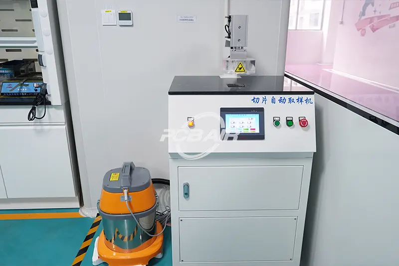
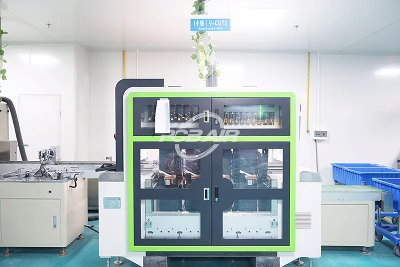
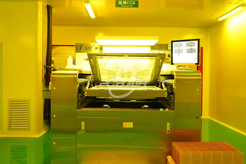
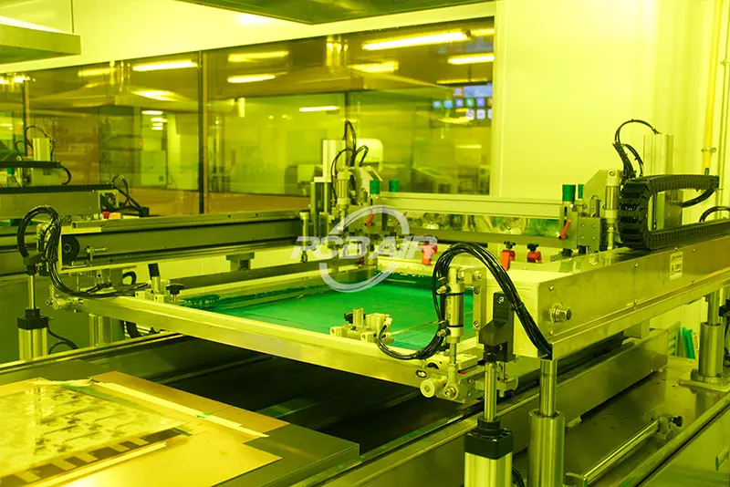
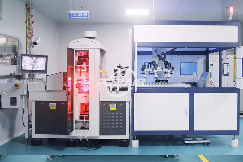
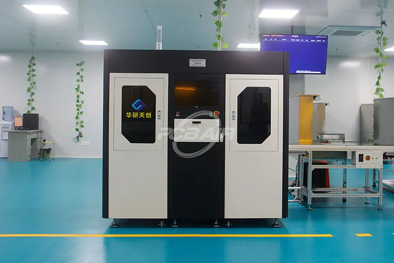
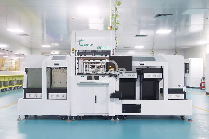
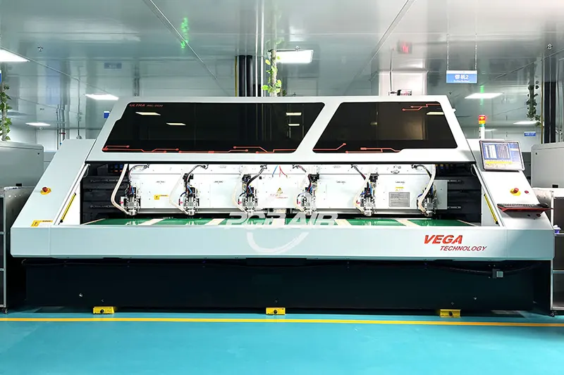
HDI PCB Manufacturing Equipment
Our 65,000 sqft campus in Shenzhen, China contains the advanced equipment required for the manufacture and assembly of your PCBs. Building HDI PCBs requires specialized equipment and processes like laser drills, plugging, laser direct imaging, and sequential lamination. HDI boards use thinner materials and feature finer lines, tighter spacing, and smaller annular rings.
Among our equipment are Laser Direct Imaging machines that provide reliable, repeatable 2/2 mils with a limited solder mask clearance of 1 mil. With this technology, we can also create probe cards, DUTs, and load boards for the semiconductor industry. If you need burn-in boards, we can produce up to 50-layer boards on a 0.276-inch thick board, featuring an aspect ratio of 40:1, metal cores, and substrate PCBs with 1.50 mil trace and space.