8:00 - 17:30
Monday to Saturday
Monday to Saturday
Heat Resistance
High Tg PCBs are heat-resistant, ideal for high-temperature environments, reducing the risk of failure during heavy thermal cycling.
Durability
Resist warping and delamination under thermal stress, enhancing reliability and longevity in challenging conditions.
Performance
Consistent electrical performance in extreme temperatures, reducing signal loss and ensuring reliability for high-frequency circuits.
High Density
High Tg PCBs are ideal for complex designs with high component density, like communication systems & automotive electronics.
Introduction to High Tg PCB
High Tg PCBs (High Temperature PCBs) are a reliable choice for high-temperature applications because they can withstand elevated temperatures without losing mechanical or electrical properties. Standard FR-4 laminates hold up to around 130-140°C. For applications that encounter higher temperatures, High Tg laminates are capable of withstanding over 170°C. In the most demanding environments, polyimide materials excel with a tolerance for temperatures exceeding 260°C. Selecting the appropriate Tg value is important to ensure your circuit board performs reliably under high-temperature conditions.
We select materials with the right Tg values for your design and application, using rigorous testing to ensure reliable PCB performance even in demanding conditions. Meanwhile, we can also provide metal-based PCBs that offer excellent heat dissipation performance, such as aluminum PCBs, LED PCBs, metal core PCBs, copper-based PCBs, and more.
High Tg PCB Manufacturing
We use inner layer, lamination, and drilling technologies to ensure the quality of our High Tg PCBs, which are made to withstand challenging high-temperature applications.
For inner layer production, we use specialized materials, including high temperature, high speed, high frequency, thick copper, and thin dielectrics, to produce high-layer count PCBs. It can be challenging to regulate signal transmission with such materials, but we address these issues effectively. As trace width reduces, risks of open or short circuits increase, potentially degrading yields. Similarly, adding more signal layers and finer traces can lead to AOI misses, especially on internal layers. Additionally, thinner inner layer dielectrics are more vulnerable to folding, leading to problems with etching quality. We combat these challenges by upgrading our equipment and using high-precision etching lines, ensuring standardized, clean etching and better quality boards.
Lamination of high-layer PCBs presents its own set of challenges, especially with thinner dielectric materials and different Tg values across multiple layers. Issues like resin cavities, bubbles, or laminate slippage can arise during the lamination process. These challenges are compounded when multiple layers are involved, making it difficult to manage expansion and contraction. We address these issues by closely monitoring the coefficients of expansion and contraction and by using software to control the lamination process. We ensure compatibility and maintain reliability even for specialized or mixed-material PCBs.
Drilling through multiple layers with high Tg, high speed, high frequency, and thick copper requires precision to prevent issues like burrs or drill bit breakage. Drilling becomes particularly challenging when there is significant copper thickness, increasing the risk of breakage. To solve this, we adjust the speed and insertion rates for each drilling point to optimize the process, and we also measure PCB expansion and contraction accurately to maintain manufacturing precision. These efforts ensure the final product is reliable, with all specifications met.
Why Choose Us as Your High Tg PCB Manufacturing Partner?
As an experienced manufacturer of high-Tg PCBs, we help you select the right laminates to match your product’s requirements. We offer high-temperature PCB solutions at competitive prices while maintaining quality and reliability. We ensure that boards are produced with strong mechanical integrity, good dimensional stability, and resistance to thermal decomposition, delivering consistent performance for your applications.
Competitive Pricing
With over 10 years in the PCB industry, PCBAIR has established a reliable supply chain that ensures access to premium components at competitive prices. For complex projects needing special materials or advanced technical specifications, our strong manufacturing capabilities enable us to provide cost-effective solutions while maintaining high quality.
Fast and Reliable Delivery
We ensure rapid production times, with samples shipped within 24-48 hours and mass production orders delivered within 72-120 hours. Our partnerships with global logistics providers like UPS, EMS, FedEx, DHL, and TNT guarantee prompt and reliable shipping, supported by our digitalized factory management and 90% automation for enhanced efficiency.
Quality Assurance
Our rigorous quality inspection begins with incoming material checks. We use AOI to detect defects and X-ray to identify internal issues. Electrical performance testing is performed with advanced automatic test machines and flying probe testers. Before shipment, our dedicated QC team conducts a thorough manual visual inspection to ensure all products meet strict quality standards.
Customer Service
Our experienced sales, order management, and engineering teams provide expert support throughout your project. The sales team handles support and project follow-ups, while the order management team ensures timely quotations and monitors production status. Our engineering team reviews your design files, offering professional advice to optimize production efficiency.
PCB Laminate Materials Suppliers
To ensure your PCBs are reliable and perform well, we use high-quality laminate materials. We have built strong partnerships with top suppliers in the industry, including trusted brands like Rogers, Panasonic, Dupont, Arlon, Taconic, Nelco, Isola, Teflon, and more. This means you receive the best materials tailored to your project needs, providing the performance and durability you expect.

High Tg PCB Capabilities
By reviewing the following high Tg PCB capabilities table, you can briefly understand what we can do.
| Specification | Capability |
|---|---|
| Base Material | ITEQ, NANYA, TUC, SYL, PANASONIC, HITACHI, Kingboard, EMC |
| Layer | 2-48L |
| Board Thickness | 0.2-8mm |
| Thickness Tolerance | ≤1.0mm: ±0.10mm, >1.0mm: ±10% |
| Minimum PCB Size | 2.5×2.5mm (need to create panel), 10x10mm (can do single board) |
| Maximum PCB Size | 500x1500mm |
| Maximum Copper | 3OZ |
| Inner Line Width and Space | 0.05/0.05mm |
| Outer Line Width and Space | 0.076/0.076mm |
| Minimum BGA Center Distance | 0.4mm |
| Mechanical Minimum Aperture | 0.15mm |
| Laser Minimum Aperture | 0.075mm |
| Finished Surface | LF HASL, plating NI/AU, plating hard Gold, ENIG, Immersion Tin, Immersion silver, OSP, ENIG+OSP, HASL+plating hard Gold, ENIG+plating hard Gold, plating gold+plating hard Gold, ENEPIG, OSP+plating hard Gold |
| Solder Mask | Green, Red, Yellow, Blue, White, Black, Pink, Purple, Matte Black, Matte Green |
| Hole Size for Machine Drill | 0.2-6.4mm |
| Shape Tolerance | ±0.10mm |
| Minimum Laser Drill | 0.075mm |
Need Help With Your Project?
Please send us a message, and our high Tg PCB manufacturing capabilities can help you complete your next project.
High Tg PCB Samples We Manufacture for Our Customers
We have obtained a variety of certifications and registrations, including ISO 9001, automotive and medical certifications, as well as SGS and UL certifications, and we maintain rigorous quality control through IQC, IPQC, and OQA. We deliver high-quality high Tg PCBs on schedule and within budget with outstanding precision.


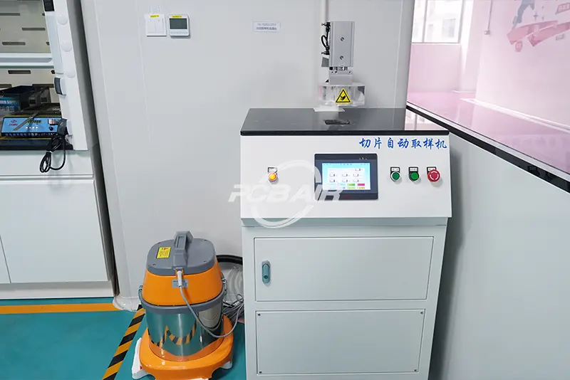
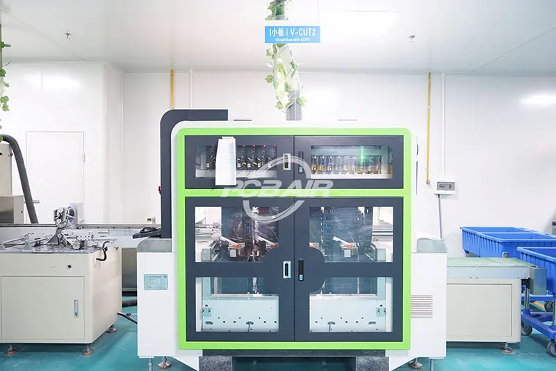
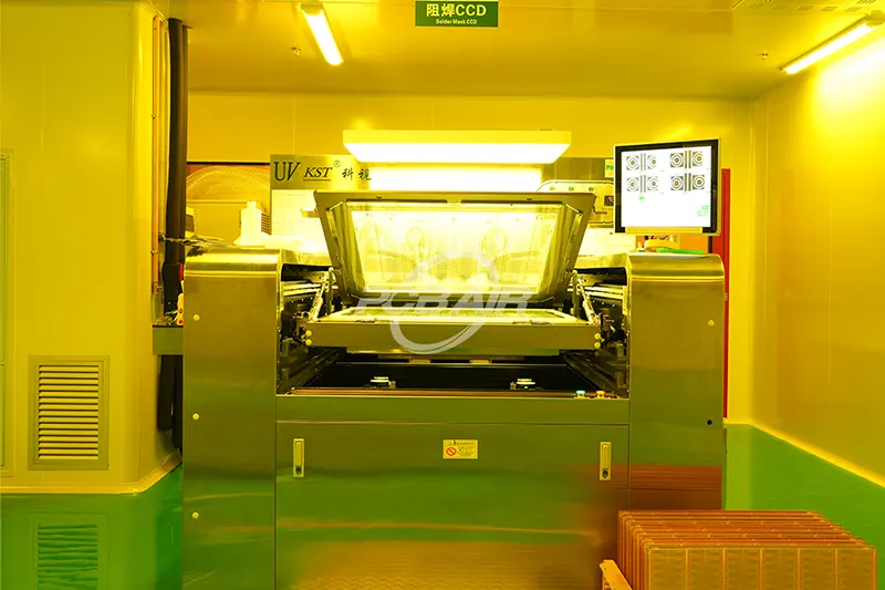
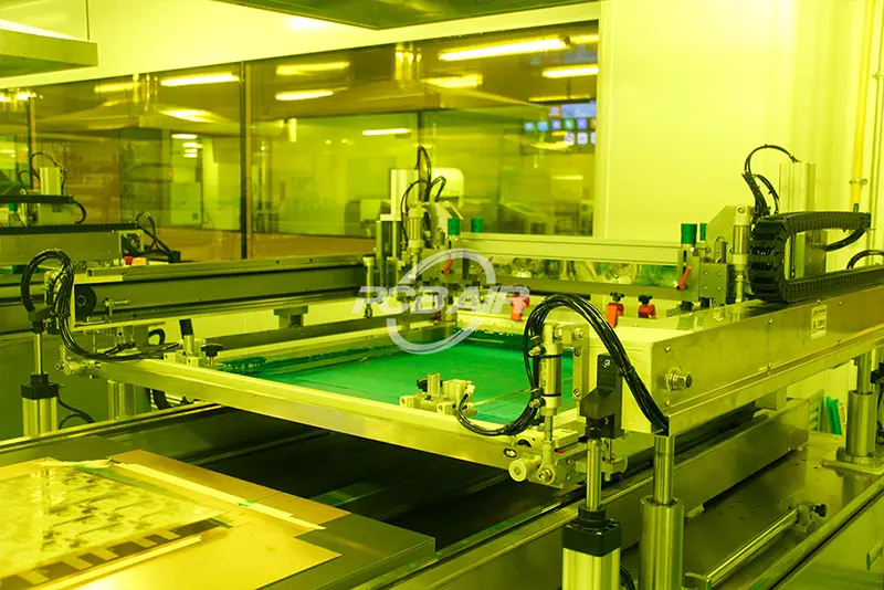
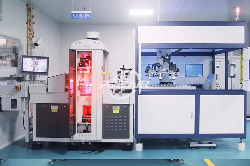
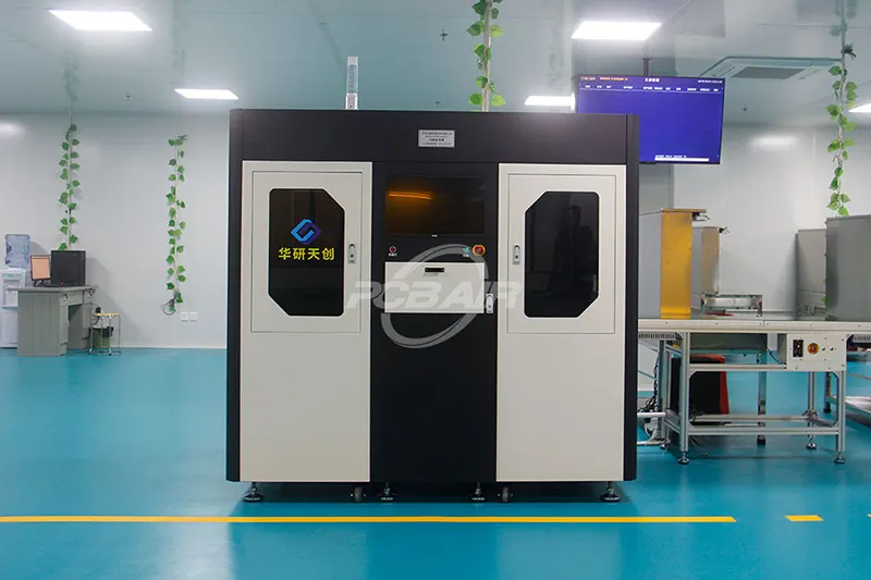
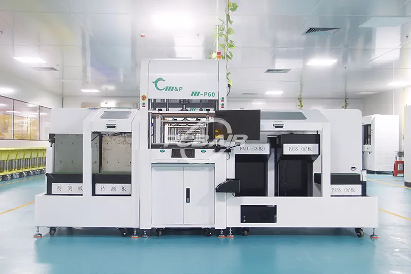
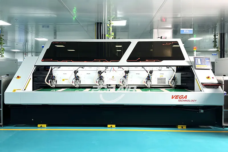
High Tg PCB Manufacturing Equipment
Our 65,000 sqft campus in Shenzhen, China contains the advanced equipment required for the manufacture and assembly of your PCBs. Our high-temperature lamination presses bond PCB layers precisely. CNC drilling machines with specialized bits create accurate holes in high Tg materials. Laser Direct Imaging systems transfer intricate designs accurately.
Advanced etching equipment and plating lines ensure precise circuits and reliable copper deposition. Solder mask application equipment and high-precision ovens provide protective coatings and proper curing. Automated Optical Inspection systems and electrical testing equipment verify each PCB meets strict quality standards.