8:00 - 17:30
Monday to Saturday
Monday to Saturday
Integrity
By controlling impedance, you reduce signal reflections and distortions, ensuring reliable data transmission and preventing data errors in high-speed applications.
EMI/RFI
Proper impedance control reduces EMI and RFI. This improves electromagnetic compatibility, so your devices are less likely to interfere with others.
Performance
Consistent signal integrity boosts your device’s performance and reliability. Impedance-controlled PCBs result in fewer errors, higher bandwidth, and longer lifespan.
Predictability
Controlling impedance gives you predictable signal behavior, simplifying design and debugging of high-speed circuits and reducing time to market.
Understanding Impedance Control
When your high-frequency signals need precise impedance control to function properly, controlled impedance PCBs become important. To keep your data intact and signals clear in high-frequency products, you need to match the impedance of PCB traces. If you don’t match the impedance to the components’ characteristic impedance, switching times increase, and your circuit experiences random errors. Who wants unexpected glitches popping up in your circuits? It’s like trying to tune into a radio station but ending up with static because the frequencies aren’t aligned.
As a manufacturer of controlled impedance PCBs, we use the Polar SI9000e impedance calculation software and precise impedance testers to meet your requirements. Before production begins, engineers simulate all impedance values based on the provided information. Once all values match, we proceed to production. After manufacturing is completed, we measure the impedance of test coupons using the impedance tester. If all impedance values fall within the acceptable tolerance of +/-5% or +/-10%, controlled impedance has been successfully achieved.
Impedance Control Layout Considerations
Impedance-controlled routing starts right at the schematic level. Specifying the values and types of your controlled impedance signals in the schematic sets the foundation for accurate routing. This clarity helps the layout team understand which nets are single-ended or differential pairs. By setting up different net classes for controlled impedance routing and annotating them on the schematic using your design tool’s rules and constraints, you streamline the entire process.
Maintaining constant impedance along a controlled trace involves several key factors. Trace geometry is one of them—the width and thickness (copper weight) of the trace directly affect impedance. Signal spacing is another crucial element. The distance between the signal trace and its return path, usually on the adjacent reference plane layer, must be carefully configured following the board layer stackup. Don’t overlook the dielectric material either. The core and prepreg materials electrically isolate the controlled impedance trace layers, and their thickness and dielectric constant play a significant role in impedance calculations.
Calculating these parameters alongside your circuit’s impedance requirements helps determine the appropriate trace width for routing. You can use trace impedance calculators built into your design tools, circuit simulators, or even online calculators and charts. These resources simplify the process and help ensure accuracy.
When you start routing controlled impedance traces in the layout, keep a few considerations in mind. Make sure to distinguish controlled impedance traces from other nets. This distinction helps the PCB manufacturer spot them easily. During manufacturing, subtle adjustments to trace widths are often necessary. If the traces aren’t easily identifiable, making these adjustments becomes more complicated. To avoid this, set up net classes in your design data or specify slightly different trace width values in the Gerber files.
For differential pairs, it’s important to route the traces parallel with consistent spacing between them. Avoid splitting the pair around obstacles like vias. Instead, arrange via fanouts to keep the lines symmetrical. This practice maintains the integrity of the differential signals.
Also, pay attention to spacing controlled impedance lines away from other objects. A good rule of thumb is to maintain a clearance of three times the trace width from nearby tracks and components. For instance, if a controlled impedance line is five mils wide, keep a 15-mil clearance to other traces and components. Setting up net classes with specific design rules and constraints can help maintain this necessary spacing automatically.
Don’t forget about clear signal return paths. Ensure that the reference planes adjacent to controlled impedance routing provide an unobstructed return path. A blocked return path is a common source of electromagnetic interference (EMI) problems in circuit boards.
To verify the integrity of your impedance-controlled designs, tools like Time-Domain Reflectometers (TDRs) and Vector Network Analyzers (VNAs) are invaluable. With these instruments, you can measure and analyze impedance discontinuities and signal reflections, ensuring that the PCB performs as intended.
Why Choose Us as Your Impedance Control PCB Manufacturing Partner?
When you need precise impedance control down to 3%, our PCB manufacturing services deliver the accuracy you require. Excelling at high-speed and high-frequency designs, we utilize materials such as FR4, ceramic, PTFE, and Metclad to meet your specific performance needs. We analyze your design data and manufacturing drawings, employing DFM tools to identify and resolve any discrepancies, ensuring your board performs as expected.
Competitive Pricing
With over 10 years in the PCB industry, PCBAIR has established a reliable supply chain that ensures access to premium components at competitive prices. For complex projects needing special materials or advanced technical specifications, our strong manufacturing capabilities enable us to provide cost-effective solutions while maintaining high quality.
Fast and Reliable Delivery
We ensure rapid production times, with samples shipped within 24-48 hours and mass production orders delivered within 72-120 hours. Our partnerships with global logistics providers like UPS, EMS, FedEx, DHL, and TNT guarantee prompt and reliable shipping, supported by our digitalized factory management and 90% automation for enhanced efficiency.
Quality Assurance
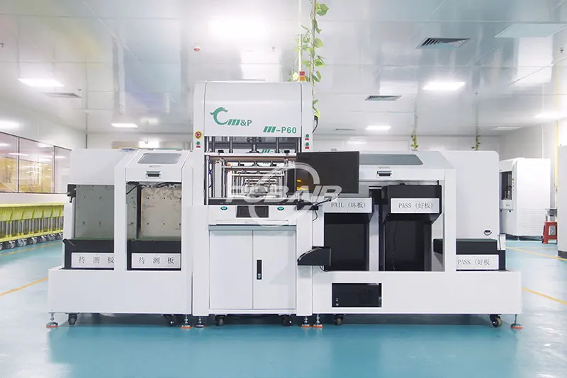
Our rigorous quality inspection begins with incoming material checks. We use AOI to detect defects and X-ray to identify internal issues. Electrical performance testing is performed with advanced automatic test machines and flying probe testers. Before shipment, our dedicated QC team conducts a thorough manual visual inspection to ensure all products meet strict quality standards.
Customer Service
Our experienced sales, order management, and engineering teams provide expert support throughout your project. The sales team handles support and project follow-ups, while the order management team ensures timely quotations and monitors production status. Our engineering team reviews your design files, offering professional advice to optimize production efficiency.
PCB Laminate Materials Suppliers
To ensure your PCBs are reliable and perform well, we use high-quality laminate materials. We have built strong partnerships with top suppliers in the industry, including trusted brands like Rogers, Panasonic, Dupont, Arlon, Taconic, Nelco, Isola, Teflon, and more. This means you receive the best materials tailored to your project needs, providing the performance and durability you expect.

Impedance Control PCB Capabilities
By reviewing the following impedance control PCB capabilities table, you can briefly understand what we can do.
| Specification | Capability |
|---|---|
| Base Material | FR4, High TG, Halogen-free, High Frequency (Rogers, Arlon, Taconic, Nelco etc.) |
| Layer | 2-36L |
| Board Thickness | 0.2-8mm |
| Thickness Tolerance | ≤1.0mm: ±0.10mm, >1.0mm: ±10% |
| Minimum PCB Size | 2.5×2.5mm (need to create panel), 10x10mm (can do single board) |
| Maximum PCB Size | 500x1500mm |
| Impedance Accuracy | ±8% (≤5Ω), ±5% (>5Ω) |
| Minimum Buried Resistance | 50Ω |
| Buried Resistance Tolerance | ±10% |
| Inner Line Width and Space | 0.05/0.05mm |
| Outer Line Width and Space | 0.076/0.076mm |
| Minimum BGA Center Distance | 0.4mm |
| Mechanical Minimum Aperture | 0.15mm |
| Minimum Laser Drill | 0.075mm |
| Finished Surface | LF HASL, plating NI/AU, plating hard Gold, ENIG, Immersion Tin, Immersion Silver, OSP, ENIG+OSP, HASL+plating hard Gold, ENIG+plating hard Gold, plating gold+plating hard Gold, ENEPIG, OSP+plating hard Gold |
| Solder Mask | Green, Red, Yellow, Blue, White, Black, Pink, Purple, Matte Black, Matte Green |
| Hole Size for Machine Drill | 0.2-6.4mm |
| Shape Tolerance | ±0.10mm |
Need Help With Your Project?
Please send us a message, and our controlled impedance PCB manufacturing capabilities can help you complete your next project.
Impedance Control PCB Samples We Manufacture for Our Customers
We have obtained a variety of certifications and registrations, including ISO 9001, automotive and medical certifications, as well as SGS and UL certifications, and we maintain rigorous quality control through IQC, IPQC, and OQA. We deliver high-quality Impedance Control PCBs on schedule and within budget with outstanding precision.


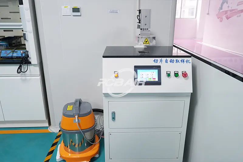
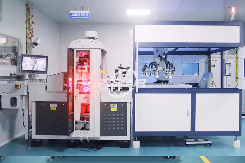
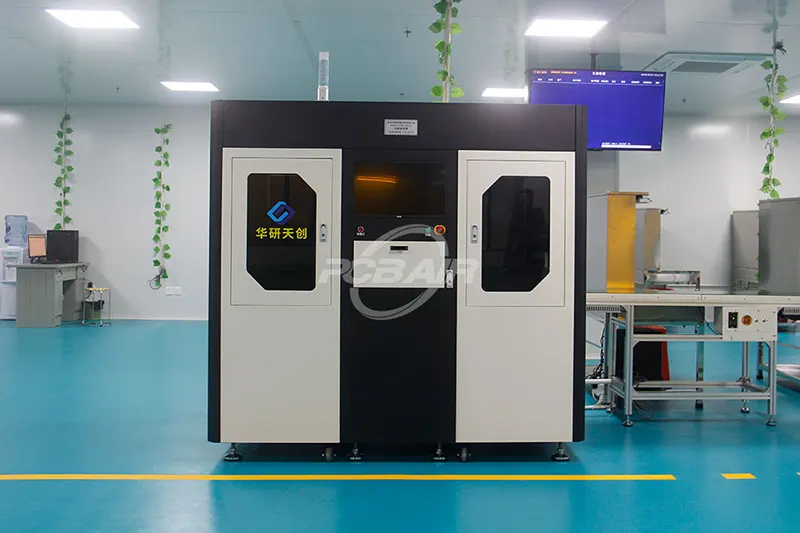
Impedance Control PCB Manufacturing Equipment
Our 65,000 sqft campus in Shenzhen, China contains the advanced equipment required for the manufacture and assembly of your PCBs. We use high-precision drilling machines and lamination presses for exact multilayer boards. LDI and photolithography equipment help create precise trace patterns needed for high-speed signal integrity.
Our electroplating and surface finish equipment provide excellent conductivity for your gold fingers. Quality is ensured with AOI systems and impedance testing equipment like TDRs. Environmental test chambers and clean rooms keep manufacturing conditions optimal.